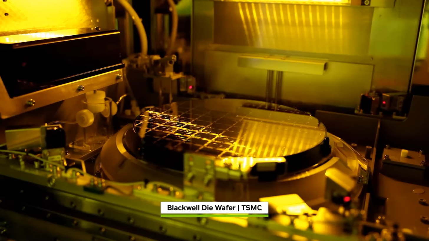
**NVIDIA Achieves First U.S.-Made Blackwell Chip Wafer, But Advanced Packaging Still Offshore**
Recently, NVIDIA made a significant milestone by announcing the successful production of the first Blackwell chip wafer on American soil. At TSMC’s Arizona facility, CEO Jensen Huang unveiled this breakthrough, marking a major achievement for the ‘Made in USA’ narrative in semiconductor manufacturing.
However, despite this progress, a crucial segment of the AI chip supply chain remains anchored overseas. Specifically, NVIDIA and its partners still rely on off-shore fabs for advanced packaging services, which are essential for transforming raw wafers into fully functional AI chips.
### What Is Advanced Packaging and Why Does It Matter?
To those unfamiliar, advanced packaging refers to the processes that follow wafer fabrication. After the Blackwell wafer is produced, it must be sliced into individual dies. Each die is then connected and mounted onto a substrate before being interconnected using cutting-edge technologies like TSMC’s CoWoS (Chip-on-Wafer-on-Substrate) or Intel’s EMIB (Embedded Multi-die Interconnect Bridge).
This packaging step is vital for scaling AI chip performance, as it stacks and integrates multiple dies with short, high-speed interconnects. Without advanced packaging, the “raw” wafer simply cannot perform as a high-powered AI processor.
### The U.S. Lags in Advanced Packaging Capacity
Currently, the United States lacks sufficient advanced packaging infrastructure. As a result, wafers produced in American fabs like TSMC Arizona are shipped back to locations such as Taiwan for the critical packaging and integration stages.
This dependency creates a supply chain constraint, adding complexity and extra costs to producing chips like NVIDIA’s Blackwell AI processors domestically.
### Industry Efforts to Bring Advanced Packaging Stateside
Recognizing this bottleneck, industry leaders are actively working to establish advanced packaging capabilities within the U.S.
TSMC has announced ambitious plans to build advanced packaging facilities as part of its multi-billion-dollar investment in the region. However, setting up such complex operations from “ground zero” will take several years.
To accelerate progress, TSMC plans to collaborate with Amkor Technology—an American company specializing in product packaging and test services. This partnership aims to offer turnkey advanced packaging solutions, including CoWoS technology, helping to speed up time-to-market for domestic chip production.
### Towards a Fully Domestic AI Chip Supply Chain
The U.S. government and industry players alike understand the importance of a comprehensive supply chain that covers both front-end wafer fabrication and back-end packaging.
With expanding investments from semiconductor giants like TSMC, the U.S. is rapidly advancing toward producing some of the world’s most powerful AI chips entirely on American soil.
While challenges remain, the successful production of the Blackwell chip wafer in the U.S. combined with ongoing efforts to build advanced packaging capabilities signals a promising future for American semiconductor manufacturing.
https://wccftech.com/nvidia-first-arizona-made-blackwell-wafer-exposes-a-hidden-weakness-the-us-can-build-chips-but-must-send-it-abroad-to-finish-the-job/